
The market is flooded with low cost smart devices, and some of them are directly tied to physical security. As we explored in a previous analysis on a smart intercom, smart locks are another category worth a closer look.
This article documents a short security analysis of one of the countless Tuya-based models available on Amazon, using it as a concrete target for hardware and firmware analysis. The techniques are standard practice in the field and the goal is not to call out a specific vendor but to take a close look at what is actually inside one of these devices: once again, the device has more to give than its manufacturer probably intended.
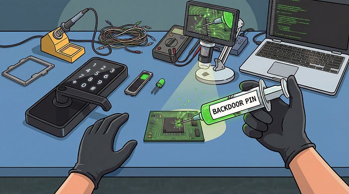
The write-up reads as a narrative following the actual progression of the analysis, from hardware inspection to firmware reverse engineering and patching to inject a persistent backdoor PIN.
Introduction
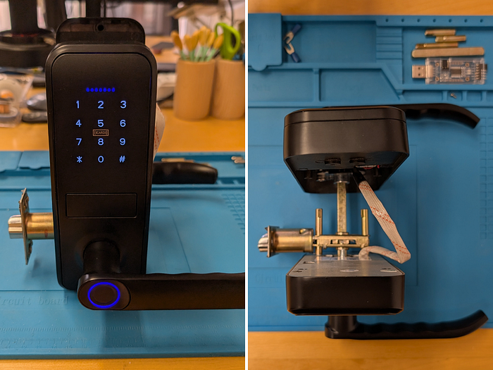
The target is a fairly typical Tuya-based smart lock: it pairs with the official Tuya mobile app over Bluetooth and supports multiple unlock methods, including permanent and temporary PINs, fingerprint recognition, and NFC tags that ship in the box. Straightforward to set up, pleasant enough to use day to day, and sitting on a desk in our office waiting to be taken apart.
In this analysis I focus on a specific slice of the attack surface: PCB and hardware inspection, debug interface analysis, firmware reverse engineering and dynamic debugging with GDB. Other surfaces were identified during the analysis (e.g. serial commands likely issued by the BLE SoC to interact directly with the lock mechanism) but are left out of scope in favor of going deeper on the firmware path and building a concrete lab exercise.
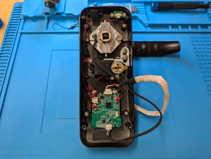
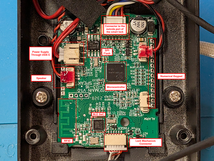
Opening the Device: PCB Analysis
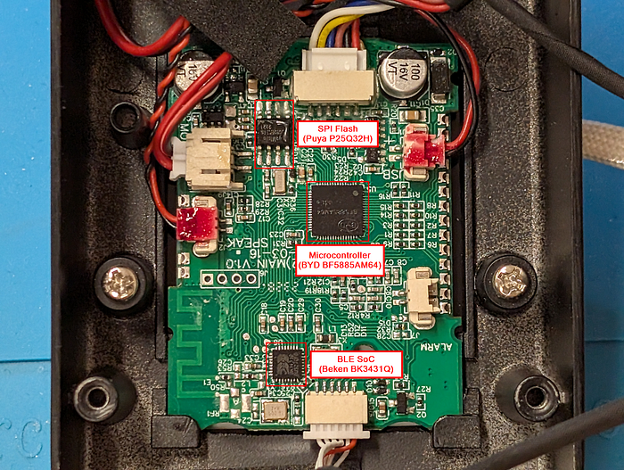
With the device open, the first focus was identifying the main components on the PCB.
Three chips immediately stood out as the most interesting targets:
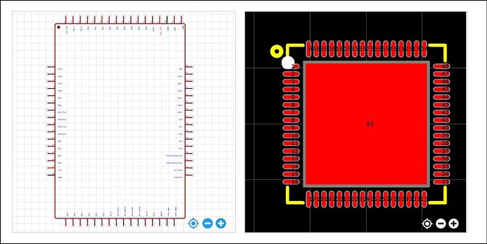
- BYD BF5885AM64: the primary microcontroller of the device, responsible for running the main application logic and managing all peripherals.
- Beken BK3431Q: a BLE SoC, most likely running the Tuya BLE SDK stack and handling Bluetooth communication with the mobile app.
- Puya Semiconductor P25Q32H: a SPI flash memory.
Gathering Documentation
The next step was collecting datasheets. For the Beken BLE SoC and the Puya SPI flash, documentation was straightforward to find online. The BYD microcontroller was a different story: no full datasheet is publicly available, something that turns out to be fairly common for chips used in low cost consumer devices from Chinese manufacturers.
The missing datasheet was a problem in particular for the pinout mapping. Knowing which pin serves which role is essential to quickly identify interfaces like SWD or JTAG, which, if left enabled by the manufacturer, would allow dumping the firmware and attaching a debugger to the device.
Without that information, the only option was to proceed in blackbox mode.
First Steps on the Board
The most obvious candidate for an SWD interface was a group of four exposed pins on the left side of the board. SWD requires four signals: VCC, GND, SWDIO, and SWDCLK. With VCC and GND straightforward to identify through basic continuity checks, only two pin combinations remained to try for the data and clock lines.
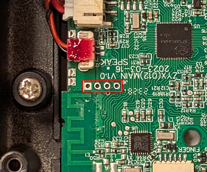
Attempting a connection through a programmer using those pins did not work. The likely missing piece was the reset pin, which is required to establish a proper SWD connection. On top of that, attaching a logic analyzer to those same pins during normal device operation revealed something that initially shifted my attention away from them: a clock signal on one pin and data on the other, consistent with I2C communication rather than SWD.
With those initial attempts exhausted, a more methodical PCB inspection eventually led to a likely reset pin candidate: grounding that pin caused the device to reboot, which was a good sign.
Around the same time, sharing the PCB details in an IoT security Discord community (IHH server by Matt Brown) turned out to be equally valuable. A community member pointed out a pinout schema for the BYD microcontroller, a resource that independently confirmed the reset pin and provided the full pin mapping that had been missing from the start.
The first Bonus section later in this article covers in more detail how I found the reset pin and the techniques that can be used to hunt for SWD and JTAG interfaces in total blackbox scenarios.
With the schema in hand, a quick continuity check with a multimeter confirmed that the four pins found earlier did indeed map to the SWD interface, most likely muxed with I2C during normal device operation, which explained the signals observed earlier.
Further useful information about the microcontroller was found directly on the official BYD website: the BF5885AM64 integrates an ARM Cortex-M0 core.

Dumping the Firmware
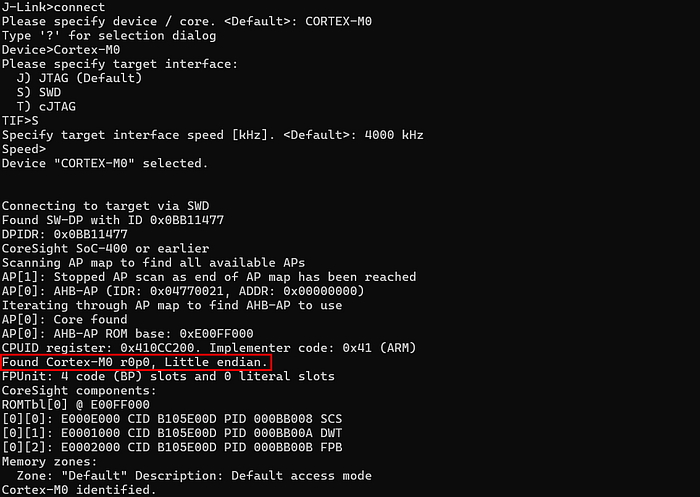
With the reset pin identified and all signals correctly connected, the programmer successfully established an SWD connection.
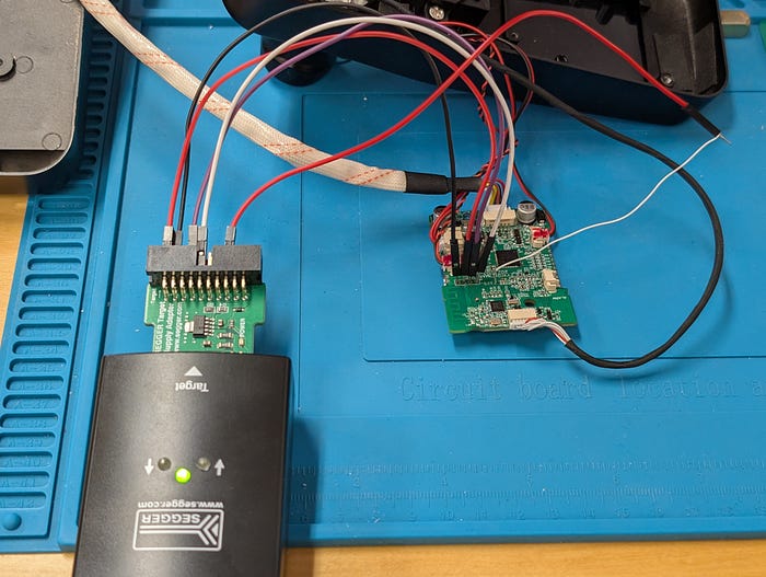
The JLink output confirmed "Found Cortex-M0 r0p0, Little endian", verifying the core architecture on the spot.
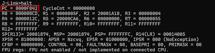
Determining the base address where the firmware was mapped was derived by cross-referencing the ARM Cortex-M0 memory map documentation with empirical observation: halting the CPU and reading the PC at 0x0000F842 confirmed that flash is mapped natively from 0x00000000, consistent with later memory probes.
With the base address confirmed, the next step was inferring the flash size. Taking the most common embedded flash sizes as reference points: 64KB, 128KB, and 256KB, I read 32 bytes near the upper boundary of each candidate range, specifically at 0x0000FF00, 0x0001FF00, and 0x0003FF00.
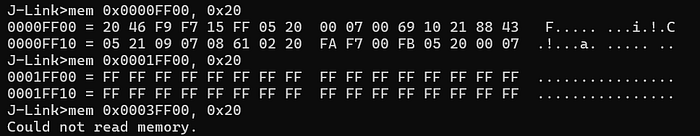
The read at 0x0003FF00 failed, ruling out 256KB. Reads between 0x0000FF00 and 0x0001FF00 returned valid opcode bytes, and reads past 0x00020000 returned no meaningful content, confirming that the internal flash is 128KB, mapped from 0x00000000 to 0x00020000.
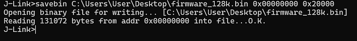
With the boundaries defined, the full firmware dump was straightforward.
With the firmware in hand, the static and dynamic analysis could begin. That part of the analysis is covered in the sections following the two bonus paragraphs below.
Bonus #1: Blind SWD Pin Enumeration
What if we're in a full black-box scenario with no datasheet, no evident target pins, nothing and we want to find debug interface like SWD? Let's see a way to approach it.
The first step is taking a closer look at the PCB and understanding how it's laid out. If the MCU pins are exposed (not a BGA package) and vias are clearly visible like in this case, we can already start excluding pins that route to other components or peripherals irrelevant to our goal, narrowing down the candidates with reasonable confidence. Below is an updated high-level map of the PCB.
Locating the RESET pin
Focusing on the pins we couldn't directly assign a role to, let's start with finding the RESET pin.
During the analysis, one resistor caught my attention: it measured around 5kΩ and had one end connected to VCC and the other to an MCU pin. This is a classic pull-up configuration, and combined with the context, it is actually indicative of a active-low reset line. More interestingly, right next to it sat a small capacitor with one end connected to the same MCU pin and the other to ground, a typical component on reset lines used to filter noise and ensure a reliable NRST signal.
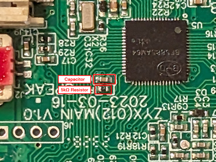
These two elements together, are a well-known fingerprint of a reset circuit, giving us already a good level of confidence.

The final confirmation came when I manually grounded the MCU pin connected to that resistor. The device immediately rebooted, observable through the keypad light pattern and the audible noise from the lock actuator. This behavioral response brings the confidence level on this being the NRST pin to pretty much certainty.
Locating the SWD pins
With the NRST pin confirmed, we can now focus on locating the SWD pins. With the PCB map in mind, we can start ruling out pins that clearly route to known components and concentrate on the ones connected to vias that terminate on pads with no obvious role, isolated or unassigned at first glance, like the ones highlighted below as an example.
To enumerate the remaining candidate pins we can leverage the methodology introduced by the JTAGulator tool by Joe Grand. In short, it works by iterating through all possible pin combinations on the target and sending protocol-specific signals, looking for valid responses that confirm the presence of a debug interface like SWD or JTAG.
Not having a JTAGulator available, there are valid open source alternatives that replicate the same approach on low cost hardware. For Arduino-based setups, SWDscan and JTAGscan are two lightweight projects that handle SWD and JTAG enumeration respectively. If you have a Raspberry Pi Pico or a Waveshare RP2040-Zero lying around, blueTag is a another valid alternative that covers both protocols.
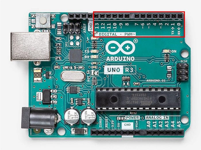
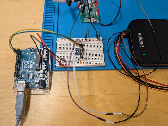
Having an Arduino Uno at hand, I went with SWDscan for the enumeration. Since the Arduino operates at 5V logic while the target board runs at 3.3V, I used a logic level shifter in between.
After flashing the SWDscan firmware onto the Arduino, the next step is defining which pins to use for the scan. This is done through a bitmask passed to the project: each bit in the mask corresponds to an Arduino digital pin, where setting a bit to 1 enables that pin for enumeration. For example, enabling pins 2 through 7 translates to a bitmask of 0xFC (binary 11111100). The firmware will then iterate through every possible combination of the selected pins, testing each pair as potential SWDCLK and SWDIO candidates.
The physical connections go from the selected Arduino digital pins through the logic level shifter, which steps the signal down from 5V to 3.3V on the target side. The output of the shifter is then connected to the PCB pads you want to probe, along with a shared GND reference.
Before probing the actual target, I wanted to verify the setup was working correctly. I connected just pins 2 and 3 to a logic analyzer with a bitmask of 0x0C, leaving the target disconnected, and captured the output.
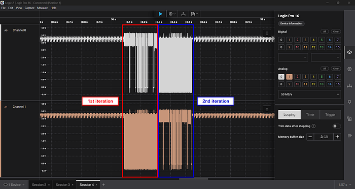
As you can see from the capture, both channels sit at around 3.3V at idle and the two possible pin combinations are clearly being tested in sequence. The setup is working as expected, so we are ready to move to the actual target.
Referring back to the PCB photo above, the group of pads highlighted in red is the one routed to the SWD interface. Four wires are connected from Arduino pins 2, 3, 4 and 5 through the level shifter directly to those pads, while the NRST pin previously identified is held low to keep the MCU in reset during the scan.
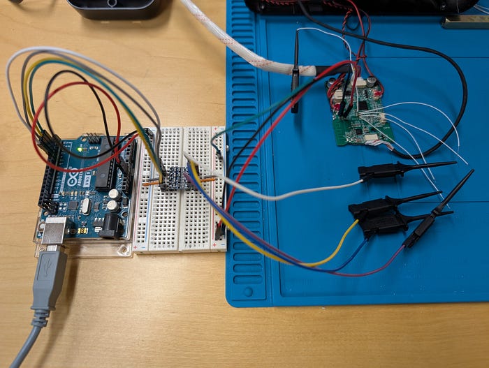
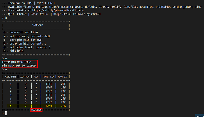
Running SWDscan with a pin mask of 0x3C (enabling Arduino pins 2 through 5), the tool finds the correct SWDCLK and SWDIO pinout after just 7 iterations.
Starting from a completely black-box scenario, PCB inspection combined with low-cost hardware and a few passive measurements can be enough to identify both the NRST and SWD pins and move forward with device and firmware investigation.
Bonus #2: What about NFC unlock method?
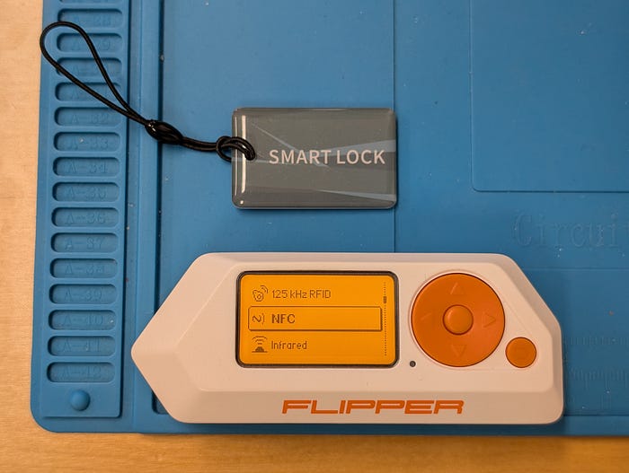
Would they have used another vulnerable MIFARE Classic NFC card? Obviously yes. As previously mentioned, the smart lock also includes NFC tags as an alternative unlock method.
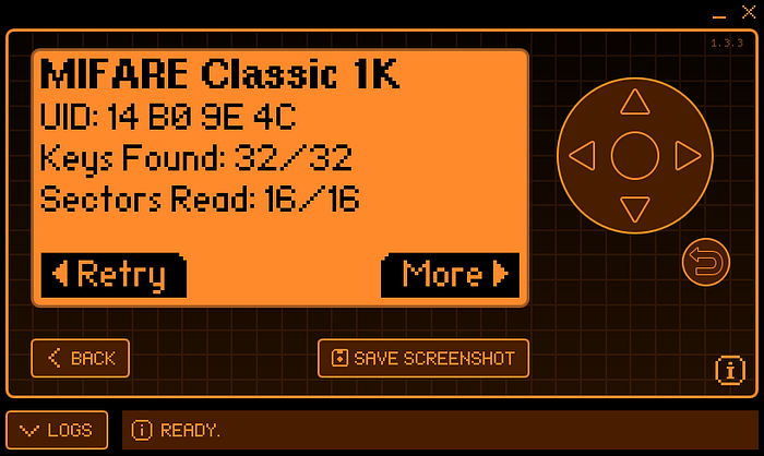
A quick scan with a Flipper Zero confirmed the tags are MIFARE Classic 1K.
MIFARE Classic cards rely on an obsolete and vulnerable encryption scheme and are subject to several well-known attacks. If you want to deep dive into the topic, here is an interesting blog post that covers it in detail.
In this case though, no attack was needed. But before jumping to the results, let's quickly recap how MIFARE Classic memory is structured.
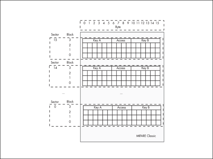
MIFARE Classic 1K memory is organized into 16 sectors, each containing 4 blocks of 16 bytes. The last block of every sector is the trailer block, which stores two keys (Key A and Key B) and the access conditions that define read and write permissions for that sector. Data is stored in the remaining three blocks. Authentication against one of the two keys is required before any sector data can be accessed.
The Flipper Zero successfully read the entire tag content, which already tells us something important: weak or default keys are in use. The dump below confirms it.
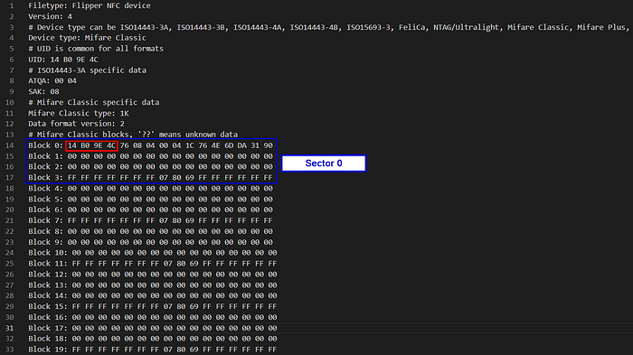
Taking Sector 0 as a reference, Block 0 is the Manufacturer Block and contains the card metadata:
- 14 B0 9E 4C: UID (4 bytes)
- 76: BCC (Block Check Character, XOR checksum of the UID bytes)
- 08: SAK (Select Acknowledge)
- 04 00: ATQA (Answer To Request Type A)
- remaining bytes: Manufacturer Data
Blocks 1 and 2 are data blocks and are completely empty. Block 3 is the sector trailer:
- FF FF FF FF FF FF: Key A (default value)
- 07 80 69: Access Bits
- FF FF FF FF FF FF: Key B (default value)
Both keys are set to the well-known default value, confirming that no custom authentication was configured. The same pattern repeats across all sectors: data blocks are empty and every sector trailer carries the same default keys.
This strongly suggests the lock implements NFC authentication purely based on Tag UID: if the UID presented by the tag matches one registered in the lock's memory, the door opens. The 4-byte UID effectively becomes the only secret, and this is one of the worst possible approaches to NFC-based access control for several reasons and mainly because:
- The UID is not protected by any cryptographic key and can be read by anyone with an NFC-capable device, including a regular smartphone
- Cloning the tag onto a writable UID card takes seconds and requires no special skills or equipment
The short video below demonstrates just how trivial the entire read and clone process is in practice.
Unfortunately, access control systems still relying on MIFARE Classic are far more common than one might expect. Beyond this smart lock, I had the chance to observe the exact same implementation on corporate building turnstiles used for employee access. In that context, after some social engineering to get close enough to a valid card for a second or two to read it, the trivial cloneability of badges made physical intrusion significantly easier during past red team engagements where that was part of the attack path.
Getting Oriented in the Firmware
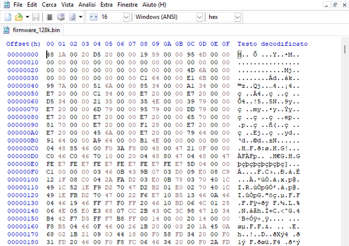
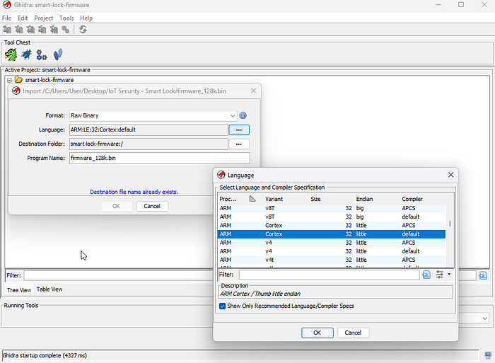
With the firmware extracted via SWD, the next step is loading it into Ghidra. The target MCU is an ARM Cortex-M0 running in little-endian mode, so I selected the corresponding processor definition at import time.
Memory map and SVD loaders
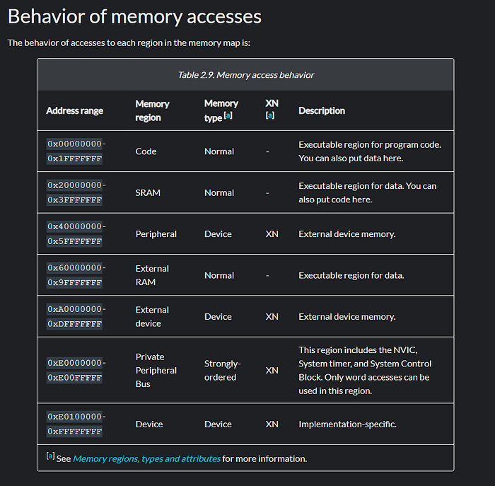
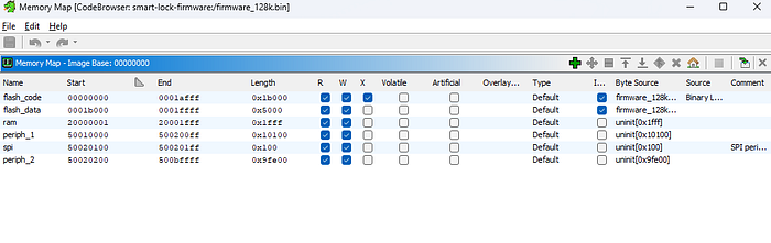
Usually, one of the first things worth doing before diving into code is giving Ghidra some context about how the address space is organized. On Cortex-M0 based microcontrollers, code, data, RAM and peripherals all live at well-defined fixed regions as documented in the official ARM Cortex-M0 memory model, which I used as a reference while setting things up.
Mapping these regions into Ghidra not only improves how it interprets code and data, but also makes reverse engineering considerably easier: when a function reads or writes to a pointer, Ghidra can label it with the corresponding region name, which gives immediate context on what is being accessed.
When a datasheet is available, the chip vendor typically publishes a more granular memory map detailing every peripheral register and memory region, its address, size and purpose. This information is often distributed in a structured XML format called an SVD file, which projects like GhidraSVD can import directly into Ghidra to automatically create named memory regions and register definitions. Unfortunately no matching SVD was available for this MCU variant, so I manually defined the main regions I could identify from the firmware itself, starting from a rough first approximation that I kept refining as the analysis progressed.
Finding the entry point
On Cortex-M0, the interrupt vector table lives at the very beginning of flash. The first word is the initial stack pointer, and the second word is the reset handler address, the actual entry point of the firmware.
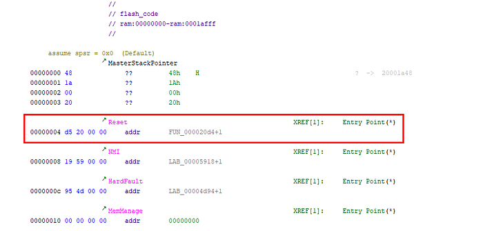
Following that address I landed in a series of function calls that looked like an initialization sequence, which eventually brought me to a function containing numerous nested calls and an infinite loop structure, the classic shape of an embedded main loop from which I continued the analysis.
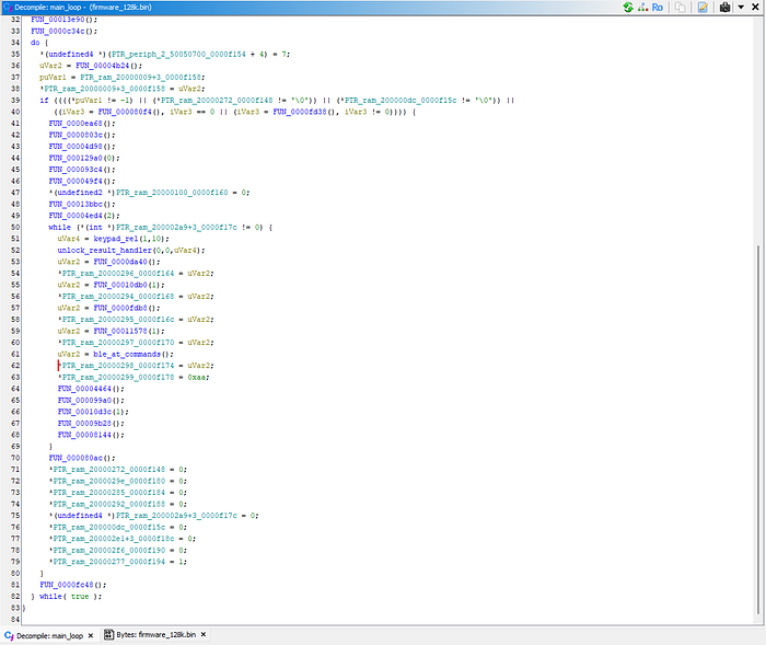
Note: During the analysis I explored more firmware functions and routines than what is shown here, but even though the approach started broad, from this point on I will focus on the routines and functions that were directly relevant to applying the firmware patch described in the next section.
Locating the credential verification function
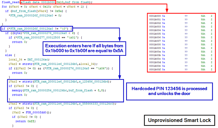
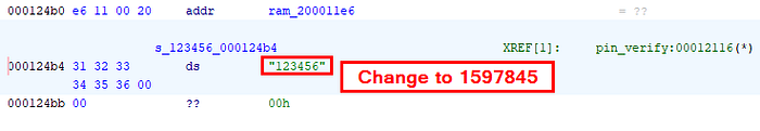
Rather than tracing every call path from the top, a faster way to reach the interesting logic is to search for meaningful strings embedded in the firmware. Browsing the string list, a cluster of numeric sequences stood out, grouped together in the same flash memory address range: "123456", "555666333", "555666111", "666888", "666777", "88991".
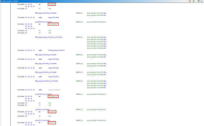
Cross-referencing "123456" led me to a single function that I initially renamed pin_verify().
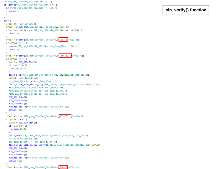
Spending some time reading through it, it became clear this was the central credential verification routine, the one the firmware calls every time an authentication attempt is made regardless of the method.
Note: The manual shipped with the smart lock listed several PIN combinations specific to the device, used for factory reset or configuration purposes. None of the sequences above appeared among them, making these undocumented hardcoded PINs left in the firmware by the developers.
Understanding provisioning
Given the PINs mentioned above I started with simple observations on how the smart lock behaves when these PINs are used. In particular let's focus on 123456. As expected on a provisioned smart lock, using that PIN results in a "Verification Failed" vocal message. Instead, after a factory reset and before pairing and reconfiguring the device, the same PIN results in "Door Unlock".
Given the pin_verify() function previously identified, this tells us that:
- There is a preliminary check to verify whether the device is provisioned or not
- If the device is not provisioned, hardcoded PINs are taken into account
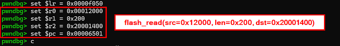
So let's see how this translates in the firmware code. At the beginning of pin_verify(), one of the first things the function does is call a routine I later renamed flash_read(), which reads a given number of bytes (param 2) from a source address (param 1) and stores them into a destination buffer (param 3).
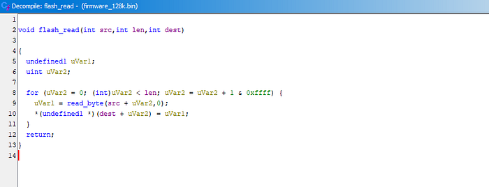
That routine is used to pull 16 bytes from address 0x1B000 and check whether all of them are equal to 0x5A. Following the code it is straightforward to see that if all 16 bytes are 0x5A, execution enters the branch where hardcoded PINs like 123456 are processed.
Given our initial observations this means: read bytes from 0x1B000 to 0x1B00F. If they are all 0x5A the device is unprovisioned and hardcoded PINs are taken into account, otherwise they are skipped entirely.
I additionally verified this by dumping the bytes at 0x1B000 to 0x1B00F while the smart lock was in a provisioned state, and they were no longer all equal to 0x5A, confirming that provisioning had modified that region.

We started this section broadly and progressively narrowed the focus down to something very specific. Given what we have seen so far, I now have everything needed to move to what the title of this article anticipated: patching the verification logic to plant a factory reset resistant backdoor PIN.
Planting a Backdoor PIN
Based on the analysis of pin_verify() we now have a clear picture of how PIN verification works in both provisioned and unprovisioned states. That understanding is exactly what we need to plant a persistent backdoor.
What to patch?
The goal is straightforward: make the firmware process the hardcoded PINs regardless of whether the device is provisioned or not, so that the backdoor PIN always unlocks the door, surviving factory resets and reprovisioning.
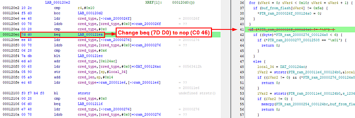
The first and main patch targets the provisioning check itself. As shown in the previous section, a beq instruction controls whether execution enters the hardcoded PIN block based on the 0x5A marker check. Converting that beq to a NOP forces execution to always fall into that block.
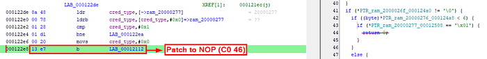
However, NOPing that branch alone is not sufficient. Through testing on the patched device I found that two additional branch instructions inside the formerly unprovisioned-only block cause early returns under certain conditions, breaking normal operation when the device is in a provisioned state. Both need to be NOPed as well to let the function behave correctly in both states.
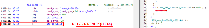
With these three patches in place the hardcoded PIN 123456 always unlocks the door regardless of provisioning state, surviving any factory reset. However 123456 is easily guessable, so the final patch replaces that string in flash with a custom less obvious value. For this exercise the backdoor PIN will be 1597845.
All of these codes are undocumented, so a victim user would have no reason to look for them or expect them to work.
How to patch?
Once I identified the bytes to change and saved the patched binary as firmware_patched.bin, the first attempt was simply rewriting the entire firmware onto the MCU internal flash using JLink. That immediately failed.
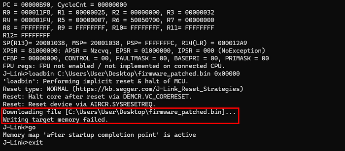
After a few more tries through gdb it became clear that direct flash writes were not possible: the flash controller required a specific unlock sequence before any write or erase operation could be permitted.
At that point I realized that the firmware itself already contained everything needed. I had already identified a flash_read(src, len, dst) function earlier in the analysis, and there had to be a corresponding write function that handled all the necessary unlock and erase steps internally. So the approach became clear: use the firmware's own flash routines against itself.
Further investigating pin_verify(), I found a function later renamed flash_write_with_hardcoded_addr that writes data to a range of addresses based at 0x1B000, an address we are already familiar with. Even though I could not use it directly because it hardcodes that base address, it contained all the building blocks needed to patch the firmware.
The high level operation is a classic read-modify-write sequence:
- Read 512 bytes from the sector-aligned flash address into RAM
- Erase the 512-byte sector just read
- Modify the target bytes in the RAM buffer at the correct offset
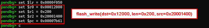
- Write the entire modified 512-byte buffer back to flash using flash_write(dst, len, src)

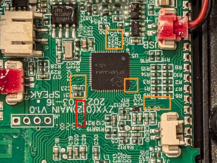
One important detail emerged during dynamic debugging: calling flash_erase() alone had no effect. Looking at the flash_erase_with_hardcoded_addr wrapper, two additional calls wrap the erase on both sides, labeled in orange in the screenshot above. Replicating that exact sequence confirmed they are required to unlock and arm the flash controller before the erase can take place, and to restore its state afterward.
Later verification through gdb confirmed that flash_erase(addr) erases 512 bytes starting from the addr passed as argument. Since the function takes no length parameter, the erase size is implicitly fixed combined with the function analysis above, I'm assuming with good confidence that the sector size is 512 bytes.
Taking inspiration from this function and using the more granular individual routines directly, the patching workflow is:
- Call flash_read(src, len, dst) to load into RAM the 512-byte sector containing the instruction or string to patch
- Modify the target bytes directly in the RAM buffer
- Replicate the full erase wrapper sequence: unlock and arm the flash controller, call flash_erase(addr), then restore the flash controller state
- Call flash_write(dst, len, src) to write the patched sector from RAM back to flash
Let's patch
With the methodology clear, it is time to control the execution flow through gdb to apply the patches and see if the device behaves as expected.
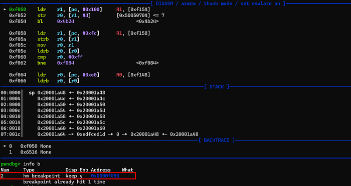
Before running any command, a small but important setup is needed. The idea is to pick a stable address inside the main loop (0x0000f050 in this case) as a fixed landing point between each operation. A hardware breakpoint is set at that address and serves as a safe pause point that the device hits every time we need to inspect state or set up the next call.
The key is the LR (Link Register): on ARM, when a function returns it branches to the address stored in LR. By setting $lr to the breakpoint address before every call, we ensure that when the invoked firmware function finishes and executes its return instruction, execution lands exactly on the breakpoint and the device halts again.
The flow for each step is therefore:
- Set $lr to the chosen breakpoint address in the main loop
- Load the function arguments into $r0, $r1, $r2 as required
- Set $pc to the target function address +1 (required on ARM Thumb to correctly branch to a function)
- Type continue so that the device executes the function and halts back at the breakpoint
- Inspect state and repeat for the next function
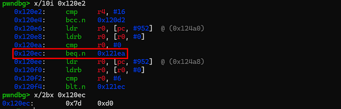
Let's now walk through the actual GDB commands for patching the beq instruction at 0x120ec.
STEP 1 — Read target sector into RAM
First, I checked the current bytes at 0x120ec and loaded the full 512-byte target sector at 0x12000 into address 0x20001400 in RAM.
0x20001400 was chosen deliberately, avoiding the lower addresses of the RAM region. Using addresses too close to the base caused unexpected corruption during testing, as some bytes in that area were being modified by the MCU when hitting the breakpoint, silently overwriting the sector buffer.
A quick dump confirmed the sector was correctly loaded, with recognizable code present at the expected offset:

STEP 2 — Patch the RAM buffer
With the sector in RAM, the target beq opcode (7D D0) was overwritten with NOP (C0 46) at the correct offset.

STEP 3 — Erase the sector
I then replicated the full erase wrapper sequence as described earlier.
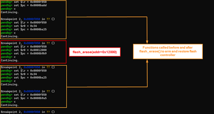
Another dump confirmed the sector was correctly erased:

STEP 4 — Write patched buffer back to flash
With the sector at 0x12000 erased and the patched buffer ready in RAM, I wrote it back to flash.
STEP 5 — Final verification
Running the same commands from the beginning confirmed the patch had been applied successfully!

The same methodology applies to all other patches listed in the previous section, which for brevity I will not show here.
Nothing left to do but see if the patched firmware behaves as expected. Below a demonstrative video of the device running it.
Once you know what to do, all these steps are easy to automate in a gdb script. That automation alone reduces the entire patching process to a matter of seconds.
This has to be intended as a lab exercise only. That said, considering that all of this could require nothing more than soldering a single wire, running a gdb script and then reassembling the device exactly as it was, I was wondering: how difficult would it actually be to sell a patched smart lock with a backdoor PIN already inside?
Conclusion
This smart lock presented itself as a modern connected security device. Under the surface it was a different story: no flash protection, NFC authentication reduced to a UID comparison, and an undocumented backdoor PIN mechanism conveniently left in the firmware.
Yet another device shipped with the debug interface enabled and no secure boot in place, and the final result is a modification that persists across factory resets without leaving any visible trace for the device owner. It is also worth noting that the near-total absence of public documentation for the MCU added friction to the analysis, but obscuring datasheets is not a security control.
What is shown here only scratches a small portion of what this device actually exposes. Much more could be uncovered with deeper research, yet even this partial analysis was enough to demonstrate an attack scenario. Devices like this continue to reach the market with little to no meaningful security validation, ending up in rental properties, shared offices, and residential buildings where users have no visibility into what they are trusting with their physical security.
Given how regulations are evolving, with the EU CRA (Cyber Resilience Act) requiring a mandatory security baseline before connected devices can be sold, a device like this one would not pass compliance after 2027.
A smart lock you cannot trust is just an expensive door handle.